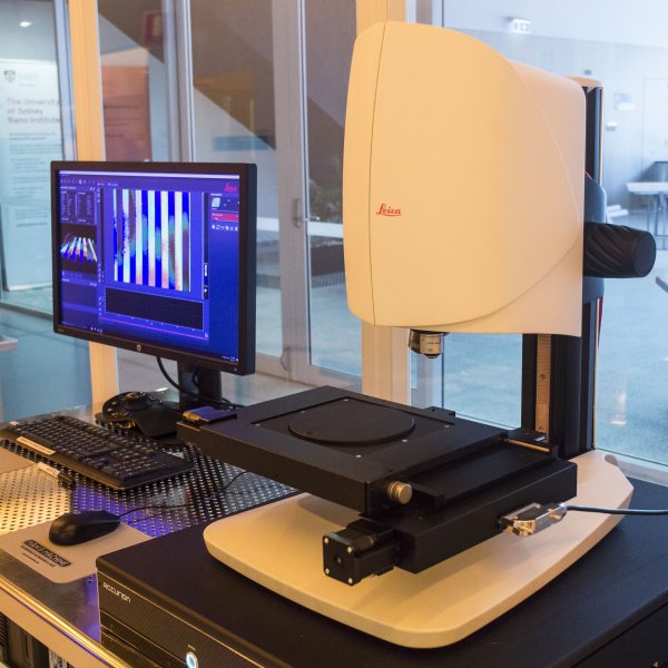
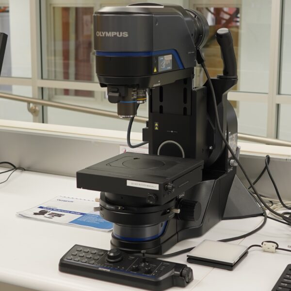
| Purpose | A metrology tool that leverages four optical modalities to image 3D topology and thin film/s properties with high automation |
| Location | Metrology Bay, RPF Cleanroom |
| Scale / volume | This microscope can accommodate samples up to 150mm diameter and 20cm in height, 3D topology mapping is limited to within a 40mm Z-range. |
| Specs / resolution | 3D topography can be mapped at a resolution down to ≈300nm in the XY plane and less than 1 nm in Z; modalities consist of confocal, three variants of interferometry, focal plane mapping, and reflectometry |
| * Not an ANFF-supported tool; access is available – refer to Access Fees schedule |
All Equipment
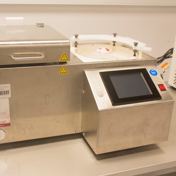
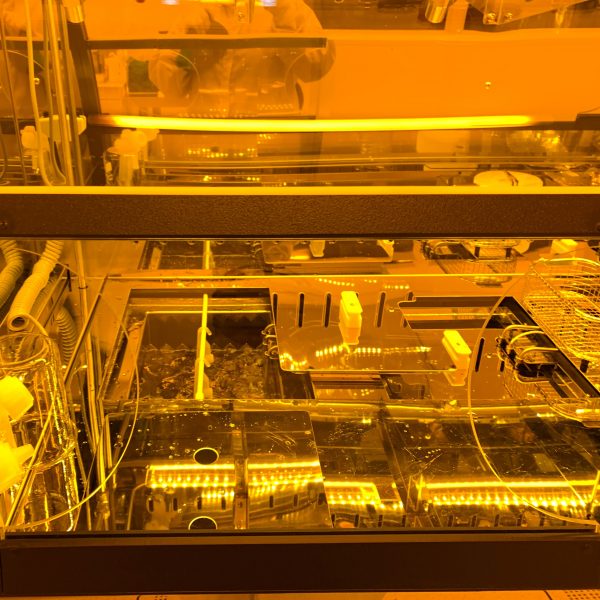
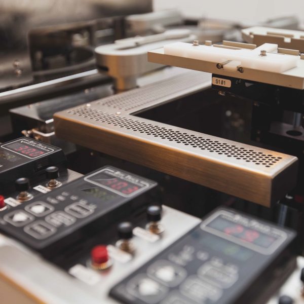
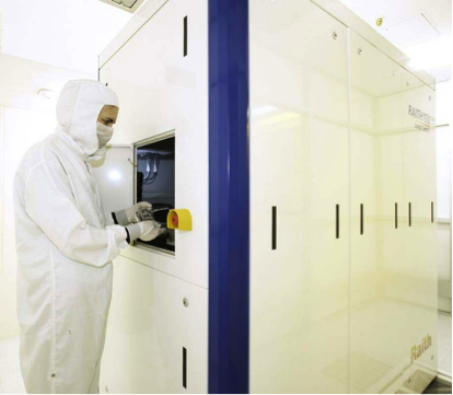
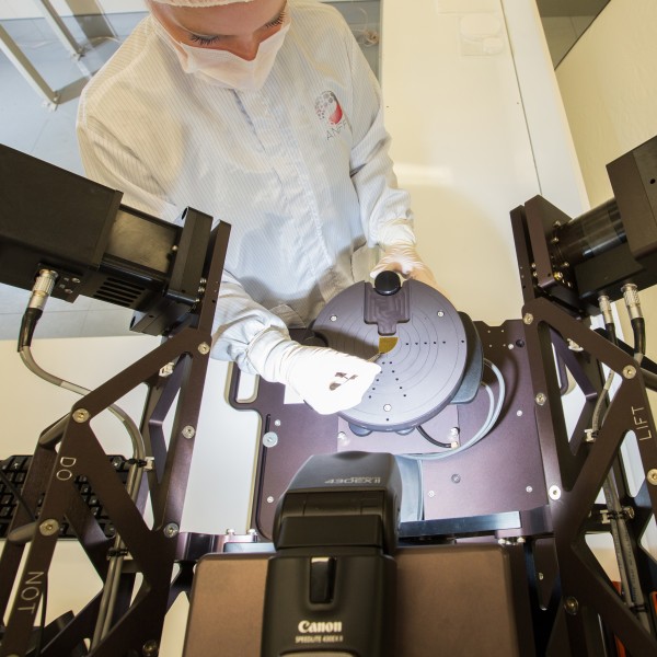
3D Microscope Leica DCM8 *
3D Printer – Filament Flashforge Creator Pro *
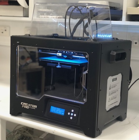
| Purpose | 3D printing of low temperature flexible materials |
| Location | RPF Madsen Lab 224A |
| Material systems | For printing Thermoplastic Polyurethane (TPU), plus other soft and flexible materials |
| Scale / volume | Maximum build area of 227mm x 150mm x 148mm |
| Specs / resolution | 120°C heating build plate; double nozzle design; has the ability to print preforms with complicated structures and then draw those into fibre whilst maintaining that structure |
| * Not an ANFF-supported tool; access is available – refer to Access Fees schedule |
3D Printer – Filament Funmat *
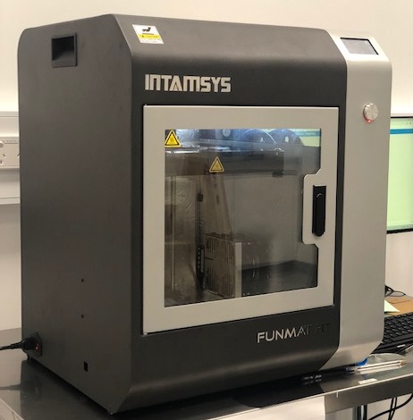
| Purpose | The Funmat HT 3D printer is fully capable of 3D printing high-performance functional materials like PEEK, ULTEM and PPSU, in addition to a broad range of engineering thermoplastics |
| Location | RPF Madsen Lab 224A |
| Material systems | Advanced thermal system design of this 3D printer includes a 90°C constant temperature chamber, up to 160°C heated build plate, and 450°C high-temperature extruder with all-metal hot end |
| Scale / volume | Build volume of the FUNMAT HT is 260mm x 260mm x 260mm |
| Specs / resolution | Users can achieve down to 50 micron high resolution industrial quality 3D printing |
| * Not an ANFF-supported tool; access is available – refer to Access Fees schedule |
3D Printer – Resin Formlabs *
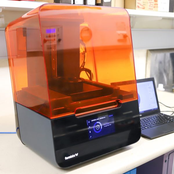
| Purpose | The Formlabs 3B SLA printer has been optimised for biocompatible materials |
| Location | RPF Madsen Lab 224A |
| Material systems | Biocompatible materials |
| Scale / volume | Build volumes of up to 14.5cm x 14.5cm x 18.5cm |
| Specs / resolution | Uses a flexible resin tank and a Light Processing Unit to produce consistent, accurate prints with X-Y resolution of down to 25µm; able to rapidly produce incredible surface finishes and high accuracy parts |
| * Not an ANFF-supported tool; access is available – refer to Access Fees schedule |
4-point Probe
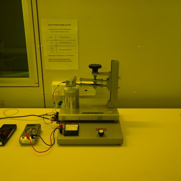
| Location | UNSW – Upper East Lab (White Area) |
| Substrates types allowed | Any |
| Substrate sizes | 30 mm x 30 mm to 2” |
| Probes | Four-point probe |
| Output | Sheet resistance for given current |
Atomic Force Microscope Bruker Icon *
| Purpose | A metrology tool that measures micron to sub-nanometre surface topology and material properties with nanometre sharp mechanical probes |
| Location | Metrology Bay, RPF Cleanroom |
| Scale / volume | This tool can accommodate 200mm wafers; maximum imaging area is 90 x 90 µm with a maximum Z-range of 10 µm |
| Specs / resolution | The resolution limit is dependent on sample and technique though generally on the order of few nm in XY and below 1nm in Z; many properties can be measured / investigated including topology, conductivity, capacitance, modulus, adhesion, etc. |
| * Not an ANFF-supported tool; access is available – refer to Access Fees schedule |
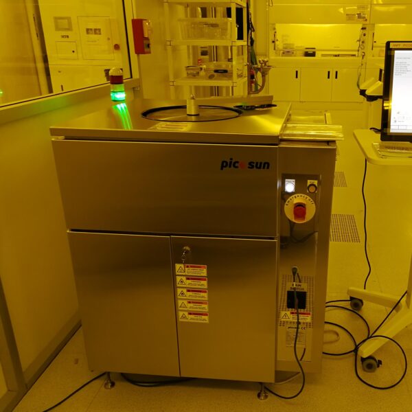
Atomic Layer Deposition Picosun R200 *
| Purpose | A thin-film deposition tool that deposits Al2O3 and HfO2 via sequential, self-limiting process cycles with precise thickness control |
| Location | Plasma Etch & Deposition Bay, RPF Cleanroom |
| Material systems | Thermal, plasma, and ozone processes |
| Scale / volume | Small pieces up to 6 inch substrates |
| Specs / resolution | Specified to be able to deposit nitrides; techniques include thermal, plasma, and ozone processes; low temperature deposition process with uniform and conformal films |
| * Not an ANFF-supported tool; access is available – refer to Access Fees schedule |
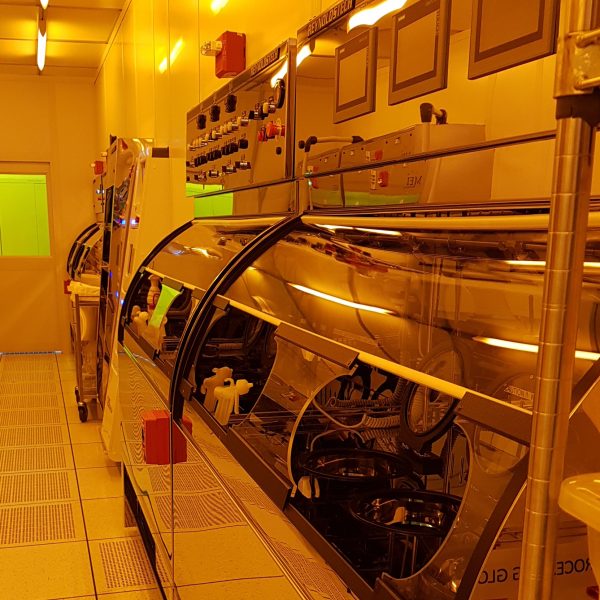
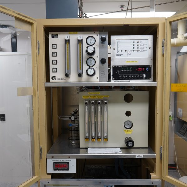
Boron Diffusion Furnace
| Location | UNSW – Upper East Lab (Grey Area) |
| Temperature range | 750 – 975 °C |
| Substrates types allowed | Si wafer, with either P or B dopants only |
| Substrate sizes | Up to 2” |
| Pre-requisites | Wafers processed in-house only, full cleaned |
| Gases available | N2 |
| Source wafers | Solid source |
Bruker Dektak XT Stylus Profiler
| Location | UNSW – West Lab (White Area) |
| Measurement Capability | Two-dimensional surface profile measurements; Optional three-dimensional measurement/analyses |
| Sample X/Y Stage | Manual 100 mm (4 in.) X/Y, manual leveling; Motorized 150 mm (6 in.) X/Y, manual leveling |
| Data Points Per Scan | 120,000 maximum |
| Max. Sample Thickness | 50 mm |
| Step Height Repeatability | 4Å, 1 sigma on steps ≤1 μm (30 scans using a 12.5 μm stylus) |
| Vertical Range & Resolution | 1 mm, 1Å (@ 6.55 μm range) |
Bruker Dimension Edge AFM
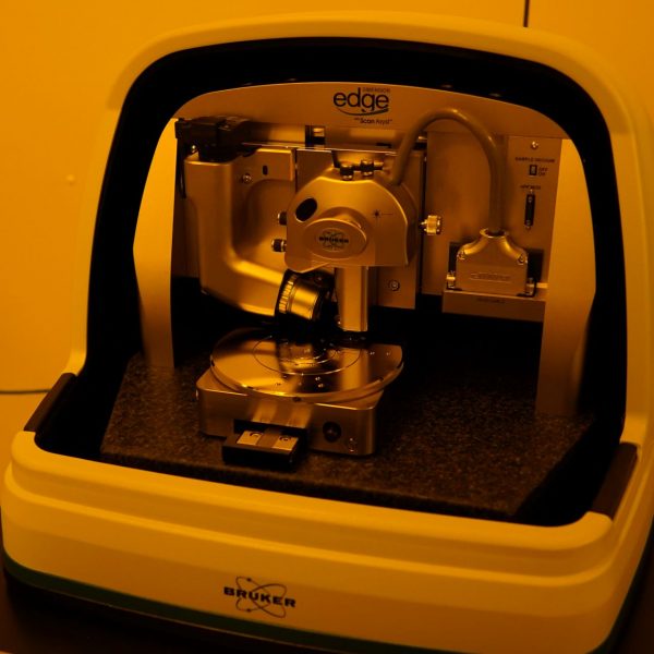
| Location | UNSW – Lower East Lab (White Area) |
| X-Y Scan Range | 90μm x 90μm typical, 85μm minimum |
| Z Range | 10μm typical |
| Vertical Noise Floor | <50pm RMS |
| Sample/Size/Holder | 150mm vacuum chuck, 15mm thick |
| Scanning modes | ScanAsyst, Tapping, Contact |
| Available tips | SNL-10, RTESP-300, SCANASYST-AIR, SCANASYST-AIR-HPI, SCANASYST-FLUID, SCANASYST- FLUID+, NCHV |
Cascade Probe Station
| Location | UNSW – South Lab (Test Area) |
| Model | Keithley Semiconductor Characterization system (4200SCS/C) |
| Available options | CV unit (4210-CVU),
Remote Preamp Option (4200-PA), Medium power SMU x 2 (4200-SMU), SMA to SSMC Dual with Local Ground (4200-PRB-C) |
Caustic Develop Wet Bench (ReynoldsTech)
| Purpose | Exhausted wet bench used for handling of caustic based chemicals – primarily TMAH based developers |
| Location | Wet Etch Bay, RPF Cleanroom |
| Material systems | Wafers and/or photomasks; TMAH based developers |
| Scale / volume | Substrates up to 7 inch square in size |
| Specs / resolution | Includes automated spin and spray process unit for development of substrates |
Chromium Etch Wet Bench (ReynoldsTech)
| Purpose | Exhausted wet bench used for handling of chromium etch chemicals |
| Location | Wet Etch Bay, RPF Cleanroom |
| Material systems | Photomask (chromium etch process); substrate (etch chromium structures) |
| Scale / volume | Etch substrates up to 7 inch square in size |
| Specs / resolution | Includes automated spin process unit |
Clean Anneal Furnace
| Location | UNSW – Upper East Lab (Grey Area) |
| Temperature range | 350 – 500 °C |
| Substrates types allowed | Si wafer, with either P or B dopants only |
| Substrate sizes | Up to 4” |
| Pre-requisites | Wafers processed in-house only, full cleaned |
| Gases available | N2, forming gas |
Clean Si Oxidation Furnace
| Location | UNSW – Upper East Lab (Grey Area) |
| Tube size | 5” tube |
| Wafer size | 2” up to 4” wafers |
| Gasses | N2, O2 |
| Temperature range | 400 – 1100C |
| Restrictions | Boron and phosphorus doped Si only |
CNT Savannah S200 atomic layer deposition system
| Location | UNSW – West Lab (White Area) |
| Materials | AlOx |
| Temperature range | 80 – 280C |
| Wafer size | Small chips up to 6” |
| Precursors | H2O, TMA |
| Restrictions | General purpose |
Coater Brewer Science CB-200
| Purpose | Spin coater for non-photo-sensitive polymer coating and baking of small samples |
| Location | RPF Lab 3021 |
| Material systems | Any material |
| Scale / volume | Can fit in up to 8 inch round wafer and 6 inch square substrate |
| Specs / resolution | The system has proximity, contact and vacuum contact baking capability |
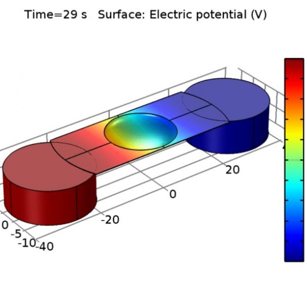
COMSOL Multiphysics
| Access mode | Remote via VPN |
| License | CPU locked |
| No of seats | 1 |
| Version | 5.1 |
| Available modules | AC/DC Module MEMS Module RF Module Wave Optics Module Heat Transfer Module Semiconductor Module Structural Mechanics Module Chemical Reaction Module Microfluidics Module Electrochemistry Module Material LibraryLivelink for MATLAB and AutoCAD |
| Hardware spec | 1500W power supply, Intel Xeon E5-2697V3 14 Core 2.6GHz CPU (x 2), DDR4 LRDIMM 32G (x 8), Leadtek quadro k620 2GB |
DMO MicroWriter ML3 Pro
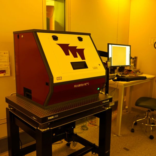
| Location | UNSW – Upper East Lab (White Area) |
| Wafer sizes | Up to 200 mm by 200 mm, 15 mm max. thickness |
| Light source | 365nm |
| Avail. resolutions | 0.5 µm, 0.7 µm, 1 µm, 2 µm and 5 µm at 365 nm |
| Greyscale levels | 256 levels |
Dektak 150
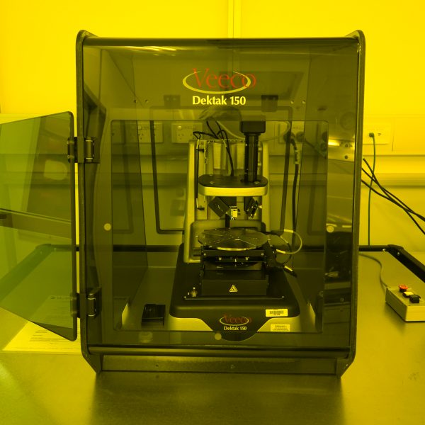
| Location | UNSW – East Lab (White Area) |
| Scan Length Range | 55 mm |
| Data Points Per Scan | 60,000 maximum |
| Max. Sample Thickness | Up to 100 mm |
| Max. Wafer Size | 150 mm |
| Height Repeatability | 6Å, 1 sigma on 1 μm step |
| Vertical Range | 524 μm |
| Vertical Resolution | 1 Å max. (at 6.55 μm range) |
| Stylus Force | 1 – 15 mg |
| Sample Viewing | 640 x 480-pixel (1/3 in.-format) camera, USB; fixed magnification, 2.6 mm FOV (166X with 17 in. monitor) |
| Sample Stage | Manual X/Y/Θ, 100 x 100 mm X-Y translation,360° rotation, manual levelling |
| Stylus radius | 6.5 µm |
Dektak 2A
| Location | UNSW – West Lab (Grey Area) |
| Sample size | From small chips up to 4” |
| Max Scan Length | 30mm |
| Max depth | 30 micron |
Dicing Saw ADT 7122 *
| Purpose | A spindle dicing system that offers customizable and/or full-automatic dicing solution |
| Location | RPF Lab 3021 |
| Material systems | Wafers, silicon, glass, ceramic |
| Scale / volume | Capable of cutting semiconductor wafers, silicon, glass, ceramic up to 6 inches |
| Specs / resolution | High accuracy up to 1µm |
| * Not an ANFF-supported tool; access is available – refer to Access Fees schedule |
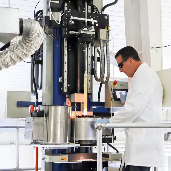
Die Bonder Fine Tech Lambda
| Purpose | The die bonder provides sub-micron precision die attach and advanced flip-chip packaging capabilities |
| Location | RPF Cleanroom |
| Material systems | Epoxy / adhesive; formic acid; thermo-compression; thermo-sonic bonding |
| Scale / volume | Heated stage accommodates up to 50mm x 50mm samples; maximum chip size for the bonder pick is 15mm x 15mm |
| Specs / resolution | Precision placement and alignment; thermo compression; ultrasonic or thermosonic bonding, formic acid, adhesive dispense module |
Dry Film Laminator Fortex FL-0305-01 *
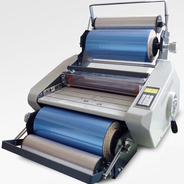
| Purpose | Uniform resist coverage and an alternative to thick liquid resist spin coating; the material feed type is an automatic roll of film and pre-cut sheets |
| Location | Photo-Lithography Bay, RPF Cleanroom |
| Material systems | Substrate material compatibility: wafers (silicon, glass, sapphire), brass, foils, steel, PCB |
| Scale / volume | Substrate thickness: up to 4mm; substrate size: from 5mm x 5mm up; 305mm x up to any desired length |
| Specs / resolution | Compatible with all dry film thickness range, but RPF stocks 50µm, 100µm, 200µm, and 500µm |
| * Not an ANFF-supported tool; access is available – refer to Access Fees schedule |
E-Beam Thermal Evaporator AJA ATC-1800-E *
| Purpose | A thin film deposition tool using e-beam or thermal process to deposit metal and oxides at nanometer scale thickness |
| Location | Plasma Etch & Deposition Bay, RPF Cleanroom |
| Material systems | Available materials include Ag, Al, Au, Cr, Ge, Ni, Ti, SiO2, TiO2, Ta2O, and Pt |
| Scale / volume | Small pieces to 6 inch substrates |
| Specs / resolution | Angled deposition capability; cooled rotating substrate holder; in-situ ion milling with Argon; controlled oxidation capability |
| * Not an ANFF-supported tool; access is available – refer to Access Fees schedule |
EBL Elionix ELS-F125 *
| Purpose | The Elionix electron beam lithography system has an acceleration voltage of 125kV and is capable of patterning high resolution features |
| Location | E-Beam Bay, RPF Cleanroom |
| Material systems | EBL resist coated wafers |
| Scale / volume | Accommodates small samples up to 6 inch wafers |
| Specs / resolution | 2nm beam diameter at 500pA beam current; dynamic focus and stigmatism adjustment; maximum 500um write field; field stitching error smaller than 20nm; overlay alignment better than 20nm |
| * Not an ANFF-supported tool; access is available – refer to Access Fees schedule |
EBL Spinner Wet Bench (ReynoldsTech)
| Purpose | Exhausted wet bench used for resist coating processes dedicated to electron beam lithography resists |
| Location | Wet Process Bay, RPF Cleanroom |
| Material systems | EBL resists |
| Scale / volume | Accommodates small samples up to 6 inch wafers |
| Specs / resolution | Includes two spinners dedicated to PMMA and CSAR / ZEP processes |
Edwards Auto 306 Thermal Evaporator (Aluminum SET)
| Location | UNSW – Lower East Lab (White Area) |
| Thin film material | Aluminium only |
| Gas | Oxygen, upper chamber for oxidation of Al only |
| Sample size | Up to 1 inch diameter (upper chamber) |
| Substrate material restriction | silicon compatible material only |
Edwards Auto 306 Thermal Evaporator (AuBe)
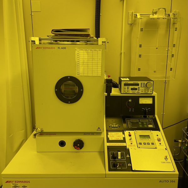
| Location | UNSW – Lower East Lab (White Area) |
| Thin film material | AuBe, Ti, Au |
| Base pressure | 9e-7 mbar |
| Sample size | Up to 3 inch in diameter |
| Substrate material restriction | Gallium arsenide compatible material only |
Edwards Evaporator
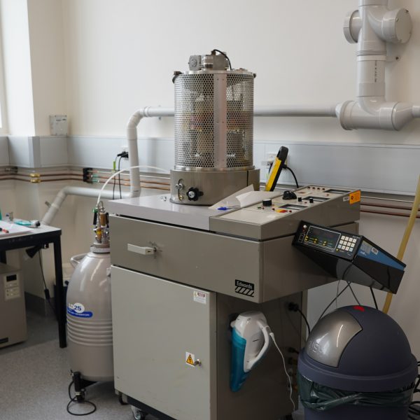
| Location | UNSW – South Lab (Test Area) |
| Maximum wafer size | 150 mm round |
| Throw | 400 mm |
| Boat contact size | 3/8” (~10 mm) |
| Maximum number of evaporator sources | 4 |
| Maximum power | 250 W |
| Additional process gases available | Ar, O2 |
| Other specifications | Glow discharge of process gases |
Electrical Probe Station Suss PM 5
| Purpose | 4 probe DC probe station for measuring electrical properties of materials and devices |
| Location | RPF Lab 3021 |
| Scale / volume | Substrate size up to 6 inch wafer |
| Specs / resolution | Can heat substrate up to 120°C during measurement |
Ellipsometer JA Woollam M2000 *
| Purpose | A metrology tool that measures the thickness & refractive index of thin films and multi-layered films using polarised light |
| Location | Plasma Etch & Deposition Bay, RPF Cleanroom |
| Material systems | Thin films |
| Scale / volume | Small samples to 6 inch wafers |
| Specs / resolution | Measurement wavelength ranges from 200nm to 1000nm |
| * Not an ANFF-supported tool; access is available – refer to Access Fees schedule |
Etch Spin Rinse Dryer (ReynoldsTech)
| Purpose | Automated batch wafer cleaning tool |
| Location | Wet Etch Bay, RPF Cleanroom |
| Material systems | Can batch process substrates in a cassette |
| Scale / volume | 2 inch, 4 inch, and 6 inch wafers; 4 inch and 5 inch photomasks |
| Specs / resolution | Can accommodate up to 6 inch wafers, interchangeable rotors |
F&S Bondtech 53XX BDA Bonder
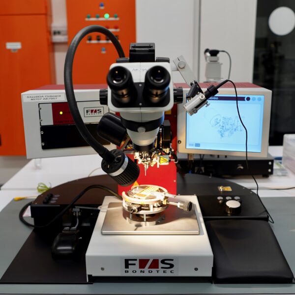
| Location | UNSW – South Lab (Test Area) |
| Configuration | 25 μ |
| Bondhead Z: | 60mm; step of 1 μm |
| Standard work height | 70mm |
| Manipulator in X and Y: | 18x18mm complies |
| Two-channel ultrasonic generator | 100-105 kHz 2.5 – 5 W |
| Wire guide | 90 °, 2 “wire coil |
Lesker Thermal Evaporator
| Location | UNSW – South Lab (Test Area) |
| Thin film material | Ge, Ni, Ti, Au, AuGe, PdAu, Cr, Al, Co |
| Base pressure | 9e-7 mbar |
| Sample size | Up to 3 inch in diameter |
| Rotation | Angled evaporation with rotation |
FIB-SEM Zeiss Crossbeam 550XL *
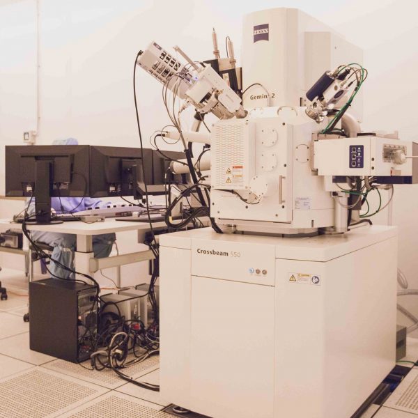
| Purpose | A multi-purpose platform that enables advanced Scanning Electron Microscopy imaging and analysis as well as Focus Ion Beam milling & deposition for cross-section profile inspection and other applications |
| Location | E-beam Bay, RPF Cleanroom |
| Material systems | It is fitted with options for elemental analysis, plasma cleaning, beam directed deposition and physical / chemical etching, diffraction based structural analysis, nano / micro manipulation, and electrical probing |
| Scale / volume | Imaging of non-conductive materials; elemental & crystallographic analysis and mapping @ ≥ 5nm; can accommodate samples as large as 150 mm wafers and 7 inch masks; 2nm image resolution; 4-10nm milling, etching, deposition |
| Specs / resolution | The FIB-SEM is a very versatile high performance tool for macro / micro / nano imaging, analysis, fabrication, manipulation, and characterisation; full analysis of any sample; in-situ milling / circuit edit / device modifications; metrology; charge compensated imaging and milling imaging; cross-sectioning; transmission imaging |
| * Not an ANFF-supported tool; access is available – refer to Access Fees schedule |
Fibre Draw Tower
| Purpose | Six meter dual sided Heathway fibre draw tower for primary and secondary drawing |
| Location | RPF Physics Lab 404 |
| Material systems | Polymers (e.g. Polyurethane, PMMA, Zeonex, Polycarbonate, TPU); soft glass (soda-lime, borosilicate, chalcogenide) |
| Scale / volume | Waveguides (solid, microstructure, air-core); co-drawn carbon elements and wires (e.g. ~500nm x 150nm wires); microstructure (internal air / fluidic channels) |
| Specs / resolution | Three furnace options for various preform sizes and temperature requirements; pressurised fibre coating system; tractor draw unit for capillary / cane drawing; pressurised drawing system; spinning motor for drawing spun fibres |
GaAs ULVAC MILA-5000 Annealing Furnace
| Location | UNSW – Lower East Lab (White Area) |
| Heating rate | 50°C/s high speed heating |
| Gas | Forming gas |
| Sample size | Up to 25 mm by 25 mm |
| Material restriction | GaAs compatible material only |
| Temperature Range | RT – 800 deg |
| Graphite plate option | Available |
General Purpose Reactive Ion Etcher
| Location | UNSW – West Lab (Grey Area) |
| Type | Parallel plate, rf |
| Target Area | 100mm |
| Substrate size | 100mm |
| Gases | Ar, O2, CF4, CHF3, SF6, (CH4 & H2 will be available soon) |
| Rf power | 200 W |
General Purpose Acid Wet Benches (ReynoldsTech)
| Purpose | Exhausted wet bench used for handling of general purpose acids |
| Location | Wet Etch Bay, RPF Cleanroom |
| Material systems | General acid chemicals; substrates |
| Specs / resolution | Includes two integrated stirring hotplates, heated and filtered process tank, and cascading tank for batch processing |
General Purpose Caustic Wet Bench (ReynoldsTech)
| Purpose | Exhausted wet bench used for handling of general purpose caustic based chemicals |
| Location | Wet Etch Bay, RPF Cleanroom |
| Material systems | General caustic / base chemicals; substrates |
| Specs / resolution | Includes integrated stirring hotplate, heated and filtered process tank, and cascading tank for batch processing |
GP Anneal Furnace
| UNSW – Upper East Lab (Grey Area) | |
| Tube size | 3” tube |
| Wafer size | Small chips up to 2” wafers |
| Gasses | N2, O2, forming gas |
| Temperature range | 200 – 1100C |
| Restrictions | General purpose |
GP ULVAC MILA-5000 Annealing Furnace
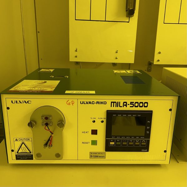
| Location | UNSW – Lower East Lab (White Area) |
| Heating rate | 50°C/s high speed heating |
| Gas | Forming gas |
| Sample size | Up to 25 mm by 25 mm |
| Material restriction | General purpose |
| Temperature Range | RT – 800 deg |
HF Constant Temperature Bath
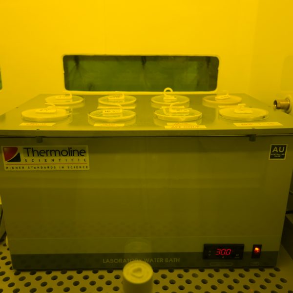
| Location | Upper East Lab (White Area) |
| Constant temperature bath | 30C |
| HF solutions available – Si/SiO2 only | HF 1:10 (HF 49% : DI water),
BHF 1:5 (HF49% : Ammonium fluoride 40%), BHF 1:15 (HF49% : Ammonium fluoride 40%) |
| HF solutions available – general purpose (GP) | BHF 1:15 (HF49% : Ammonium fluoride 40%) |
HF Wet Bench (ReynoldsTech)
| Purpose | Exhausted wet bench used for handling of hydrofluoric acid |
| Location | Wet Etch Bay, RPF Cleanroom |
| Material systems | Hydrofluoric acid |
| Scale / volume | Small samples up to 4 inch wafers |
| Specs / resolution | Includes heated process tank and cascading tank for rinsing |
Hotplate Tower (ReynoldsTech)
| Purpose | Exhausted stacked hotplates for baking during solvent based processes |
| Location | Wet Process Bay, RPF Cleanroom |
| Material systems | Resist baking |
| Scale / volume | Accommodates small samples up to 6 inch wafers |
| Specs / resolution | Includes 6 hotplates dedicated to different temperature ranges – used for baking / outgassing purposes |
IBS Ion Implanter
| Location | UNSW – Far East Lab |
| Ion energy | 25-200 keV (single charge) |
| Ion current | Greater than 1 mA (typically ~100s uA) |
| Species | P, B, Sb, Ar, H, N |
| Substrate size | Max 6” wafer |
| Substrate carrier | 4 positions |
| Substrate angle to beam | Normal or 7° |
ICP RIE Oxford Plasmalab 100 *
| Purpose | A dry etching tool that etches Si and Si-based materials with an inductive-coupled plasma source in the process chamber |
| Location | Plasma Etch & Deposition Bay, RPF Cleanroom |
| Material systems | Available gases are SF6, C4F8, CF4, CHF3, supported with argon, oxygen, and helium |
| Scale / volume | Either 4 inch or 6 inch carrier |
| Specs / resolution | Cryo processes; pseudo Bosch; resist masks; in-situ optical monitoring for etch stop |
| * Not an ANFF-supported tool; access is available – refer to Access Fees schedule |
Jipelec RTA
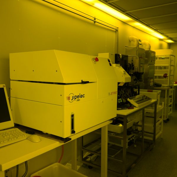
| Location | UNSW – Upper East Lab (Grey Area) |
| Temperature range | 400 – 1050 °C |
| Substrates types allowed | Si wafer, with either P or B dopants only |
| Substrate sizes | Up to 4” |
| Pre-requisites | Wafers processed in-house only, full cleaned |
| Gases available | N2 |
K and S Al Wedge Bonder
| Location | UNSW – South Lab (Test Area) |
| Wire material | Al, 25 microns diameter |
| Bonding modes | 45 deg, manual, semi-automatic (Z-axis) |
Karl Suss Manual Wafer Scriber
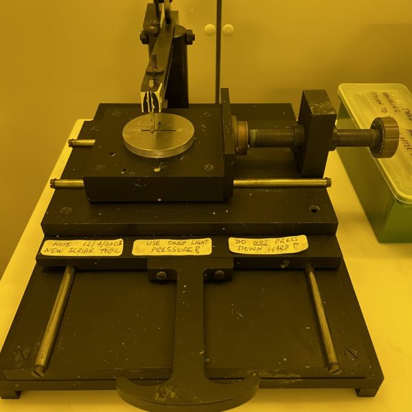
| Location | UNSW – Upper East Lab (White Area) |
| Wafer size | Small pieces up to 100 mm |
| Scriber tip | Diamond tip |
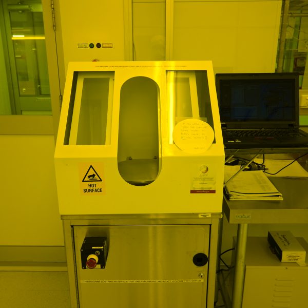
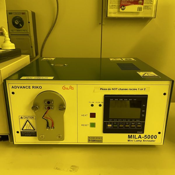
Lamp Annealer ULVAC MILA 5000 *
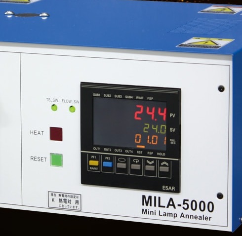
| Purpose | A desktop annealer capable of delivering high speed heating and cooling |
| Location | Wet Etch Bay, RPF Cleanroom |
| Material systems | Gases available N2 and forming gas |
| Scale / volume | Maximum wafer size 20mm x 20mm |
| Specs / resolution | Maximum temperature of 1000°C; 50°C/s high speed heating |
| * Not an ANFF-supported tool; access is available – refer to Access Fees schedule |
Laser Cutter Universal VLS3.60 *
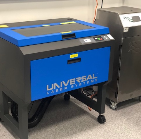
| Purpose | The Universal VLS3.60 laser cutter is a high performance, floor-standing platform manufactured in the USA and comes with a powerful 50 watt CO2 laser system |
| Location | RPF Madsen Lab 224A |
| Material systems | The VLS3.60 laser cutter is gas assist capable and has been designed for high material throughput producing high accuracy parts. |
| Scale / volume | The machine has a materials processing area of 610mm x 305mm x 229mm |
| Specs / resolution | The machine is paired with Coreldraw2019 software for optimum design capability and ease of use; the VLS3.60 capable of cutting extruded acrylic sheet up to 12mm thickness |
| * Not an ANFF-supported tool; access is available – refer to Access Fees schedule |
Laser Writer Heidelberg DWL 66+
| Purpose | Direct write laser lithography system capable of high resolution and grayscale patterning; UV laser direct-write system at submicron resolution for quick prototyping |
| Location | Photo-Lithography Bay, RPF Cleanroom |
| Material systems | Photoresist coated substrates with up to 6mm thickness |
| Scale / volume | 375nm laser wavelength; accommodates up to 9 inch wafers; |
| Specs / resolution | 800nm; maximum write area 200mm x 200mm; multiple write modes – capable of achieving submicron features with highest resolution |
Mask Aligner EVG 610 *
| Purpose | A photolithography tool that supports top and back sides mask alignment and can pattern with feature size in micron; vacuum contact, soft contact, proximity exposure modes |
| Location | Photo-Lithography Bay, RPF Cleanroom |
| Material systems | Photomasks and photoresist-coated substrates |
| Scale / volume | Photomask sizes: 4 inch, 5 inch, and 7 inch; substrate size: 2 inch, 4 inch, and 6 inch |
| Specs / resolution | Vacuum contact: 1 – 1.5um; soft contact: 1.5 – 3um; proximity: >3um |
| * Not an ANFF-supported tool; access is available – refer to Access Fees schedule |
Maskless Aligner Heidelberg MLA100 *
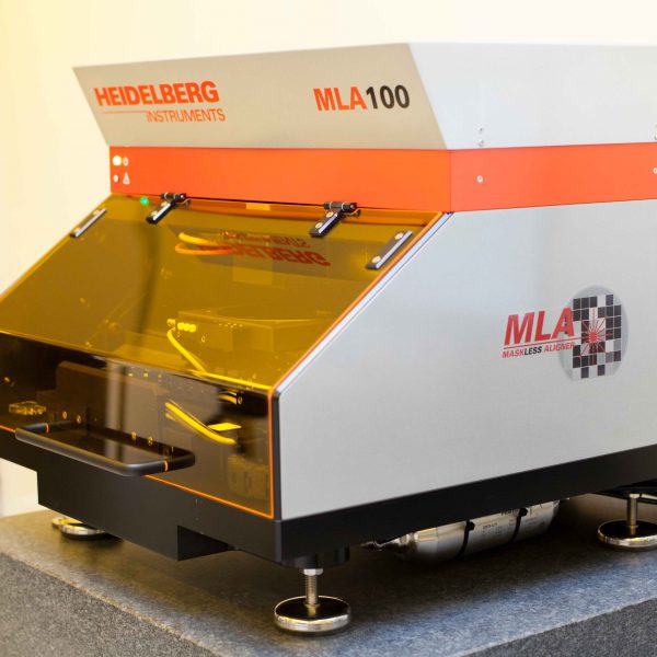
| Purpose | A fast-speed maskless alignment photolithography tool that patterns feature size down to 2um; UV LED direct-write system for feature sizes at the micron level |
| Location | Photo-Lithography Bay, RPF Cleanroom |
| Material systems | Photoresist coated substrates with up to 6mm thickness |
| Scale / volume | 365nm LED wavelength, fast writing speed; accommodates up to 6 inch wafers |
| Specs / resolution | 2um; maximum write area is 125mm x125mm |
| * Not an ANFF-supported tool; access is available – refer to Access Fees schedule |
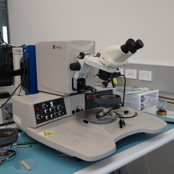
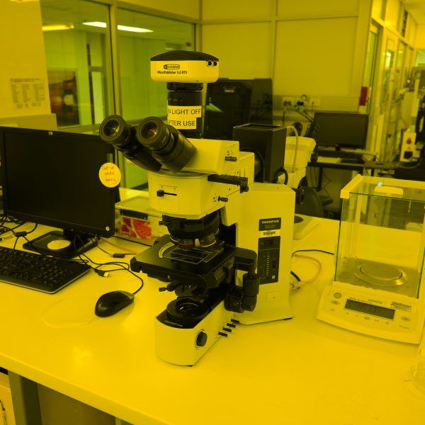
Microscope Nikon Eclipse LV100ND
| Purpose | A manual upright optical microscope with NIS Software and UV source |
| Location | Metrology Bay, RPF Cleanroom |
| Scale / volume | Can accommodate up to 150mm wafers |
| Specs / resolution | Combined reflectance / transmitted illumination with brightfield, darkfield, DIC, fluorescence, polarising, and phase-contrast; resolution limit is ≈300nm |
MJB3 Mask Aligner
| Location | UNSW – Lower East Lab (White Area) |
| Sample holder size | From small chips up to 3” wafers |
| Mask holder size | 4” square |
| Exposure modes | Vacuum, soft contact, hard contact |
| UV lamp spec | 365nm, 10 mW/cm2 |
Muffle Furnace
| Location | UNSW – South Lab (Test Area) |
| Working volume | 3.5 L |
| Temperature range | 50 – 1000°C |
| Gases | N2 |
NanoFab Helium Ion Beam Zeiss *
| Purpose | A metrology and fabrication tool that enables imaging and fabrication at resolutions below what is possible in scanning electron microscopes |
| Location | RPF HIM Suite |
| Scale / volume | Sample sizes are limited to 50mm diameter and 30mm height |
| Specs / resolution | It is fitted with components for imaging non-conductive materials, nanoscale milling / deposition, and circuit editing; image resolution is ≈0.5nm, with ultimate limits of ≈1.5nm to 5 µm for milling / deposition |
| * Not an ANFF-supported tool; access is available – refer to Access Fees schedule |
NMP Bath (photomask cleaning)
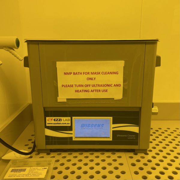
| Location | UNSW – Lower East Lab (white area) |
| Constant temperature bath | NMP at 80C |
| Other capabilities | ultrasonic |
| Mask size | up to 5” |
O2 Plasma Asher Glow *
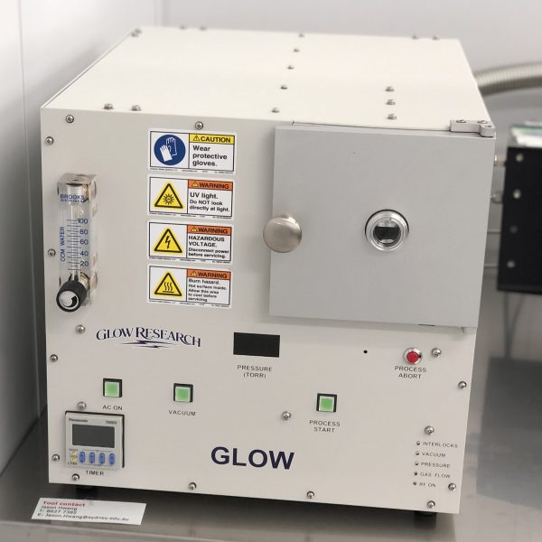
| Purpose | A small plasma system that provides O2 plasma surface treatment such as wafer cleaning and photoresist / organic removal |
| Location | Plasma Etch & Deposition Bay, RPF Cleanroom |
| Material systems | Available gas is oxygen |
| Scale / volume | 10cm x 10cm samples |
| Specs / resolution | 50W RF power |
| * Not an ANFF-supported tool; access is available – refer to Access Fees schedule |
OEG MR200 diamond scriber
| Location | UNSW – South Lab (Test Area) |
| Wafer size | Small pieces up to 200 mm |
| Scriber tip | Diamond tip |
Olympus BH2 Microscope
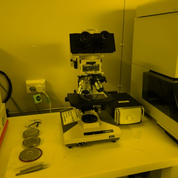
| Location | UNSW – Lower East Lab (White Area) |
| Sample size | From small chips up to 4” |
| Objective magnifications | 5X, 10X, 20X, 50X, 100X |
| Features | Nomarski DIC Prism available on 50X objective |
Olympus BX51 Phase Contrast & Darkfield Microscope
| Location | UNSW – West Lab (White Area) |
| Sample size | From small chips up to 4” |
| Objective magnifications | 5X, 10X, 20X, 50X, 100X |
| Features | Darkfield & Phase Contrast |
Optical Microscopes Olympus DSX 510 *
| Purpose | A semi-automated upright digital optical microscope with LED light source |
| Location | Metrology Bay, RPF Cleanroom |
| Scale / volume | Can accommodate up to 150mm wafers with 100mm x 100mm addressable area |
| Specs / resolution | Reflectance illumination with brightfield, darkfield, DIC, and polarising; resolution limit is ≈300nm |
| * Not an ANFF-supported tool; access is available – refer to Access Fees schedule |
Olympus DSX1000 Digital Microscope
| Location | UNSW – West Lab (Grey Area) |
| Features | BrightField, Oblique Illumination, Darkfield, MIX Illumination, Polarization, Differential Interference Contrast Motorized XY stage, Tilting Frame including motorized Z |
| Avail. Magnifications | Zoom 140X-1400X, 30mm working distance, N,A. 0.3 Zoom 560X-5600X, 4.5 working distance, N.A. 0.8 Zoom 42-420X (long working distance) |
Parylene Coater
| Location | UNSW – South Lab (Test Area) |
| Sample type | ALL (but contamination or hazardous ones) |
| Sample size | Up to 6” wafer (4 tiers substrates holder) |
| Adhesion promoter | Silane A-174 |
| Thickness range | 100 nm to 10um
(Thicker layer on request) |
| Dimer type | Parylene C |
PDMS Process Tools
| Purpose | Casting PDMS devices from a master to replicate features up to nanoscale |
| Location | RPF Lab 3021 |
| Material systems | Master material can be silicon, glass, aluminium, plastic, or polymer based substrate |
| Scale / volume | Throughput is up to one 4 inch device per hour |
| Specs / resolution | Can replicate features from 300nm and above |
PDMS Station
| Location | UNSW – Lower East lab (Grey Area) |
| Silicon Elastomer | Sylgard 184 (Dow Corning) |
| Thickness Range | PDMS membranes (10-500um)
PDMS blocks (1-10mm) |
Phosphorus Diffusion Furnace
| Location | UNSW – Upper East Lab (Grey Area) |
| Temperature range | 800 – 955 °C |
| Substrates types allowed | Si wafer, with either P or B dopants only |
| Substrate sizes | Up to 2” |
| Pre-requisites | Wafers processed in-house only, full cleaned |
| Gases available | N2 |
| Source wafers | Solid source |
Photo Spinner Wet Bench (ReynoldsTech)
| Purpose | Exhausted wet bench used for resist coating processes dedicated to thicker photolithography based resists |
| Location | Wet Process Bay, RPF Cleanroom |
| Material systems | Substrates to be coated with photoresist |
| Specs / resolution | Includes three spinners dedicated to positive, negative, and thick resist processes |
Picosun R-200 ALD system
| Location | UNSW – West Lab (White Area) |
| Materials | HfO2 and Al2O3 |
| Substrate | Small chips to 200mm |
| Temperature Range | 100C – 500C |
| Precursors | H2O, TMA and TEMAH |
Process Spin Rinse Dryer (ReynoldsTech)
| Purpose | Automated batch wafer cleaning tool |
| Location | Wet Process Bay, RPF Cleanroom |
| Material systems | Can batch process substrates in a cassette |
| Scale / volume | 2 inch, 4 inch, and 6 inch wafers; 4 inch and 5 inch photomasks |
| Specs / resolution | Can accommodate up to 6 inch wafers, interchangeable rotors |
Reactive Ion Etcher (Plasmatherm Vision) *
| Purpose | A compact reactive ion etching tool |
| Location | Plasma Etch & Deposition Bay, RPF Cleanroom |
| Material systems | Available gases are SF6, CF4, CHF3, supported with argon, oxygen, helium and nitrogen |
| Scale / volume | Accommodates 6 inch wafers |
| Specs / resolution | Optical emission spectroscopy endpoint detection |
| * Not an ANFF-supported tool; access is available – refer to Access Fees schedule |
Reactive Ion Etcher (South Bay RIE3000)
| Purpose | Reactive ion etch system dedicated to oxygen and argon plasma processes |
| Location | Plasma Etch & Deposition Bay, RPF Cleanroom |
| Material systems | Available gases are argon and oxygen |
| Scale / volume | Accommodates 6 inch wafers |
| Specs / resolution | Used primarily for resist and sample cleaning |
Solvent Develop Wet Bench (ReynoldsTech)
| Purpose | Exhausted wet bench used for solvent based development processes |
| Location | Wet Process Bay, RPF Cleanroom |
| Material systems | Solvents |
| Scale / volume | Accommodates small samples up to 6 inch wafers |
| Specs / resolution | Includes cold plate for cold development processes |
Solvent Lift-off Wet Bench (ReynoldsTech)
| Purpose | Exhausted wet bench used for solvent based metal lift-off and cleaning processes |
| Location | Wet Process Bay, RPF Cleanroom |
| Material systems | Substrates |
| Specs / resolution | Includes 3 heated ultrasonic tanks, an ambient filtered tank, and a cascading tank |
Spin coater (lower east)
| Location | UNSW – East lab (White Area) |
| Sample size | Small chips up to 4” wafers |
| Spin speed | Up to 8000 rpm |
Spin Coater (West white)
| Location | UNSW – West Lab (White Area) |
| Sample size | From small chips up to 6” |
| Max spin speed | 10k rpm |
| Max acceleration | 7300 rpm |
| Recipes | Multistep user programmable recipes |
Spin Dryer Delta 15
| Purpose | An automated single wafer substrate cleaning tool using DI water and compressed air |
| Location | Wet Process Bay, RPF Cleanroom |
| Scale / volume | 4 inch and 6 inch wafers; 4 inch, 5 inch, 6 inch, and 7 inch photomasks |
Sputter Coater DC Emitech K550
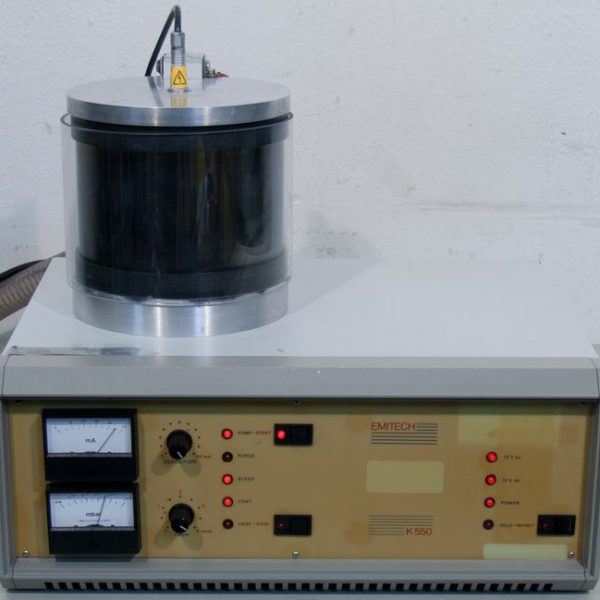
| Purpose | A small DC sputtering tool that can coat metal onto substrate |
| Location | Plasma Etch & Deposition Bay, RPF Cleanroom |
| Material systems | Available metal targets include Au, Ti, and Ni |
| Scale / volume | Small pieces to 6 inch substrates |
| Specs / resolution | Multiple small substrates for coating; coating uniformity up to 3.5 inch diameter |
Sputterer AJA ATC-2000-UHV *
| Purpose | A 5-gun DC/RF sputtering system that deposits metal and oxides at a controlled angstrom per second rate |
| Location | Plasma Etch & Deposition Bay, RPF Cleanroom |
| Material systems | Available materials include NbTi(N), SiO2, TiO2, ITO, Al, and Ti |
| Scale / volume | Small pieces to 6 inch substrates |
| Specs / resolution | Base pressure lower than 5 x10⁻⁸ torr; in-situ ion milling available; RF biased sample pre-clean available; substrate rotation with heating up to 800oC; ion milling / assisted deposition with Argon; controlled oxidation or nitration capability |
| * Not an ANFF-supported tool; access is available – refer to Access Fees schedule |
STS ICP-DRIE
| Location | UNSW – West Lab (Grey Area) |
| ICP Power | 1800 W |
| Target power | 600 W |
| Gases | Ar, O2, CHF3, CF4, SF6, C4F8, He |
| Bosch process | YES |
| Substrate size | 4” |
| Electrostatic Clamp | YES |
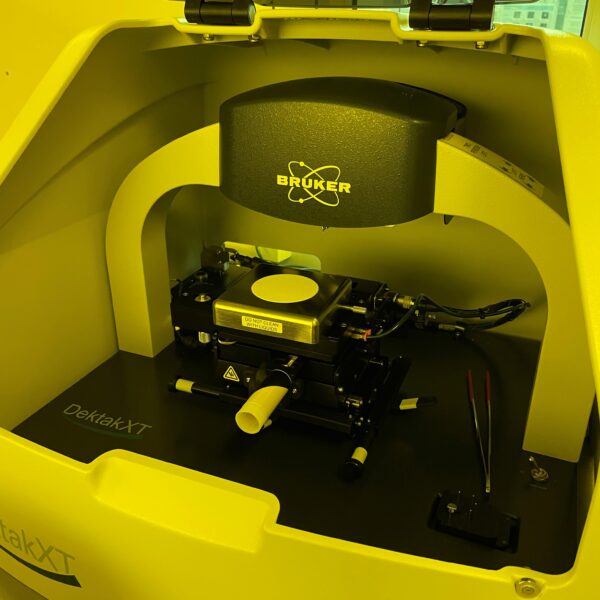
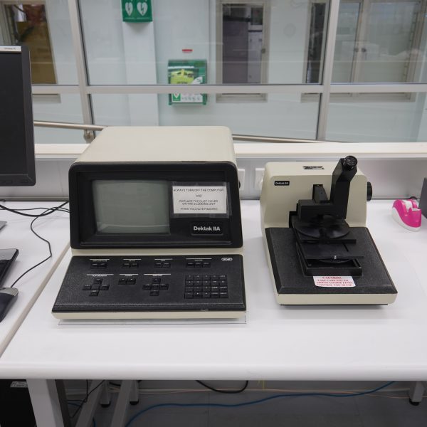
Stylus Profilometer DekTak XT *
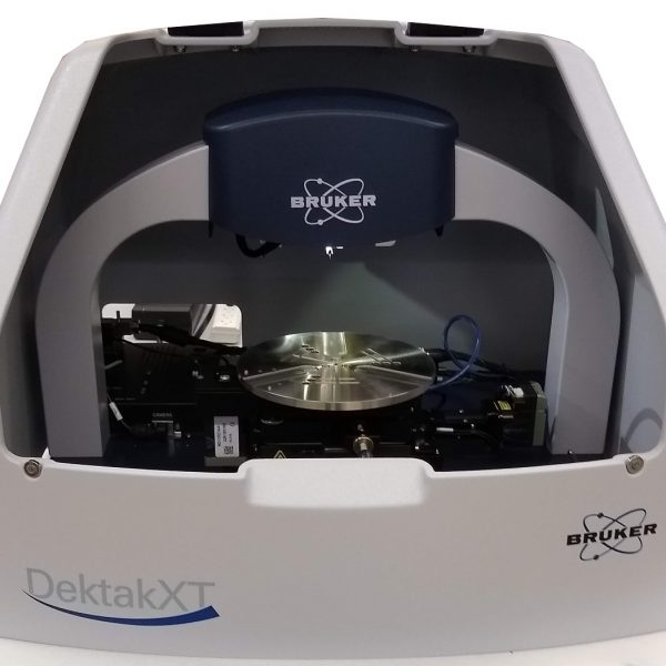
| Purpose | The Dektak XT profilometer is a stylus profiler capable of measuring step heights, film stress, and surface roughness |
| Location | Metrology Bay, RPF Cleanroom |
| Scale / volume | Can accommodate up to 150mm wafers |
| Specs / resolution | This tool is generally used for measuring 2D profiles and has a 0.1nm vertical resolution |
| * Not an ANFF-supported tool; access is available – refer to Access Fees schedule |
AlphaPlasma Asher
| Location | UNSW – West Lab (White Area) |
| Sample size | From small chips up to 8” |
| Chamber diameter | 235 mm |
| Microwave power | 2.45 GHz adjustable between 50 – 1200 watts |
TPT HB10 Thermosonic Au Ball Bonder
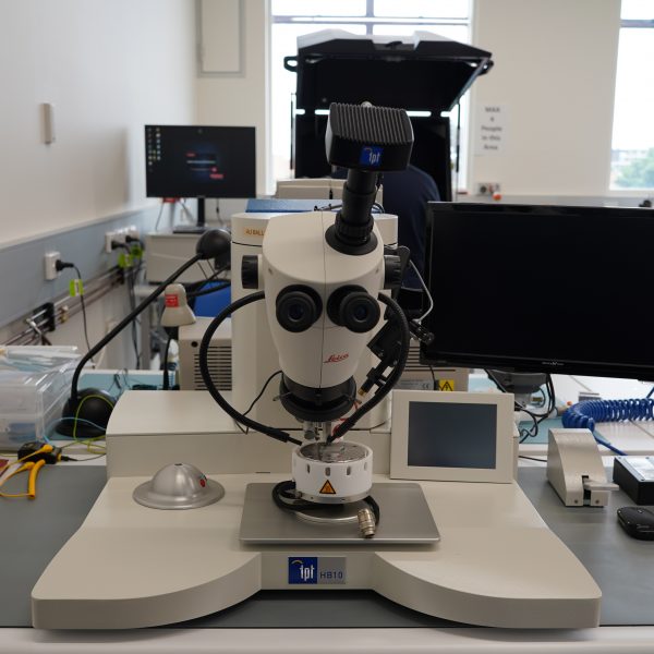
| Location | UNSW – South Lab (Test Area) |
| Wire material | Au, 25 microns diameter |
| Bonding modes | Manual, semi-automatic (Z-axis) |
| Options | Laser marker, video camera |
Tystar Mini-Tytan Horizontal 3 Stack LPCVD Furnace System
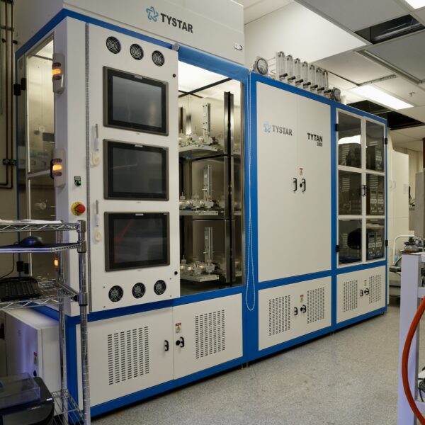
| Location | UNSW – East Lab (Grey Area) |
| Max capacity | 50 x 8” wafers per run, though typically 25 x 6” or 4” |
| Tube #1 | Stoichiometric and Low-Stress nitride |
| Tube #1 gases | Dichlorosilane (DCS), Ammonia (NH3), Nitrous Oxide (N2O) |
| Tube #2 | P-doped or intrinsic polysilicon, amorphous silicon, dry oxide, low temp oxide P-doped or undoped. (Dopant gas currently unavailable) |
| Tube #2 gases | Silane (SiH4), Boron Trichloride (BCl3), Oxygen (O2) |
| Tube #3 | N-doped or intrinsic polysilicon, amorphous silicon, dry oxide, low temp oxide P-doped or undoped. (Dopant gas currently unavailable) |
| Tube #3 gases | Silane (SiH4), Phosphene (PH3), Oxygen (O2) |
| Temperature range | 400C – 950C (recipe dependent) |
| Pressure range | 100 mTorr – 500 mTorr |
UDOX Furnace
| Location | UNSW – Upper East Lab (Grey Area) |
| Temperature range | 800 – 1000 °C |
| Substrates types allowed | Si wafer, with either P or B dopants only |
| Substrate sizes | Up to 2” |
| Pre-requisites | Wafers processed in-house only, full cleaned |
| Gases available | N2, ultra-dry oxygen |
Wafer Track Processor Rite Track SVG88
| Purpose | A fully automated system for spin coating, HMDS application, baking, and development |
| Location | Photo-Lithography Bay, RPF Cleanroom |
| Material systems | Auto dispense of resist – standard SPR660, and another type; MF26 developer |
| Scale / volume | Throughput of up to 60 wafers per hour; accommodates 3 inch, 4 inch and 6 inch wafers |
| Specs / resolution | Capable of running 25 wafers at a time; the system is well suited to batch scale production, providing high process performance and consistency in coating and development |
Wire Bonder TPT HB 100 *
| Purpose | The TPT wire bonder is capable of performing automatic and semi-automatic wire bonding with gold and aluminium wires |
| Location | RPF Lab 3021 |
| Material systems | Samples on PCB |
| Specs / resolution | Capable of manual, semi-auto and auto mode; wedge and ball bonding; deep access bond head |
| * Not an ANFF-supported tool; access is available – refer to Access Fees schedule |
Veeco Gen930 III-V MBE
| Location | UNSW – South Lab |
| Purpose | epitaxial growth of III-V materials |
| Material systems | III-V semiconductors |
| Source materials | Ga, In, Al, As, Sb, Bi |
| Dopant materials | Si, Be |
| Scale/volume | wafers up to 75mm diameter |
Pascal pulsed laser epitaxial system
| Location | UNSW – South Lab |
| Purpose | materials scouting via epitaxial growth techniques |
| Substrate materials | wide range of substrate materials |
| Target materials | LiCoO3, Li3PO4, LiCoO2, VO2, VO3, MoO3, BNBTMn, LSMO, SrTiO3, LaAlO3, SrRuO3, SAO, LLTO, LAO, BTO, LCMO, STO, SrRuO3, NGO, ZMO, BCZT, BSZT, Sm2O3, LNMO, LTO, Cr2O3, Sr3Al2O6 |
| Scale/volume | Single wafers up to 25mm diameter |
| Specifications | 248 nm excimer laser. Max energy 400 mJ per pulse, avg power 8 W. Typically energy used ~100 mJ , In-situ reflective high energy electron diffraction (RHEED). Substrate temperatures up to 1000C |
Raith 150TWO Electron Beam Lithography System
| Location | UNSW – West Lab (White Area) |
| Sample size | From small chips up to 6” |
| SEM | ZEISS |
| Column | Gemini 0-30kV |
| Apertures | 7.5 10 15 20 30 60 120micron |
| FBMS | Available |
| Laser Height Sensing | Available |
| Focusing during exposure | By Column or by Stage Adjustment |
| Stitching Write Fields capability | Available |
| Smallest step size | 2nm |
| Beam shape | Spot |
| Minimum feature size | < 20nm |
| EBL resists available | Positive PMMA 950k, CSAR 9% and 18%, negative Ma-N2403 |
| Detectors | In-lens and SE |
Raith Pioneer TWO
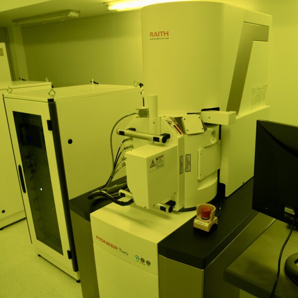
| Location | UNSW – West Lab (White Area) |
| Sample size | From small chips up to 2” |
| SEM | ZEISS |
| Column | Gemini 0-30kV |
| Apertures | 7.5 10 15 20 30 60 120micron |
| Laser Height Sensing | Available |
| Focusing during exposure | By Column or by Stage Adjustment |
| Stitching Write Fields capability | Available |
| Smallest step size | 2nm |
| Beam shape | Spot |
| Minimum feature size | < 8nm |
| EBL resists available | Positive PMMA 950k, CSAR 9% and 18%,
negative Ma-N2403 |
| Detectors | In-lens and SE |
Karl Suss MA6 mask aligner
| Location | UNSW – West Lab (White Area) |
| Light source illumination | i-line (365nm) |
| Light Intensity | 10 mW/cm2 |
| Resolution | Down to 1 um
(depends on substrate size and flatness, resist type and thickness, and cleanroom conditions, and therefore, might vary for different processes) |
| Substrate size | Pieces from 5x5mm2, to 6” wafer |
| Photomask size | 4”, 5” and 7” |
| Exposure modes | Contact (Soft, Hard, Vacuum, Low vacuum)
Flood exposure |
| Alignment method | Top Side alignment (TSA)
Bottom Side alignment (BSA) |
Lesker PVD75 e-beam evaporator - Si-MOS compatible
| Location | UNSW – West Lab (Grey Area) |
| Sample type | Silicon Only – Si-MOS Compatible |
| Sample size | Up to 4” wafer |
| Material available | Ti, Al, Pt and Pd |
| Thickness range | 1nm to 500nm |
| Option | Plasma clean capability by Ar sputtering |
Lesker PVD75 e-beam evaporator - general purpose
| Location | UNSW – West Lab (Grey Area) |
| Sample type | ALL (but contamination or hazardous ones) |
| Sample size | Up to 6” wafer |
| Material available | Metals: Ag, Al, Au, Co, Cr, Cu, Fe, Ge, Ir, Nb, Ni, NiFe, Pd, Pt, Si, Sn, Ti
Oxides: Al2O3, CeO2, Fe2O3, In2O3, SiO2, TiO2, WO3 Other materials by prior approval |
| Thickness range | 1nm to 500nm (Thicker layer on request) |
HHV sputtering system
| Location | UNSW – West Lab (Grey Area) |
| Sputter gases | Ar, N2, O2 |
| Target materials (3” targets) | Ti, Al, Cr, Au, Cu, W, Nb, Ag, Si, ITO, Si3N4, SiO2, TiO2, ZnO |
| RF power | 600W max |
| 2000W max | |
| Chamber heating | Room Temp to 400 |
| Max sample size | 6” |
| Base pressure | Mid 10-8 mtorr |
Oxford Instruments Plasmalab 100 plasma-enhanced chemical vapour deposition system
| Location | UNSW – Upper East Lab (Grey Area) |
| Materials | SiO2, SiN, a-Si:H |
| Temperature range | 100 – 300C |
| Wafer size | Small chips up to 6” |
| Gasses | SiH4, NH3, N2O, N2, Ar, CF4 |
| Restrictions | no metals |
Oxford Instruments Plasmalab 100 Reactive Ion Etching System
| Location | UNSW – Upper East Lab (Grey Area) |
| Sample size | From small chips up to 6” |
| Gases | SF6, CF4, CHF3, O2, Ar,C4F8, N2 |
| RF power | 0-300W |
| Processes available | Si deep and shallow, SiO2, SiNx, Ge, Al2O3 |
| Process Pressure range | 5-250mTorr |
| Chiller temperature range | 0-80°C |
| DC range | 0-500V |
J A Woollam spectroscopic ellipsometer
| Location | UNSW – West Lab (Grey Area) |
| Modes | Spectral ellipsometry, transmission measurements |
| Wavelength range | 200 – 1000nm |
| Spot size | 3x3mm |
| Stage | No scanning |
| Wafer size | Small chips up to 6” |
| Software | WASE, Complete EASE |
Oxford PlasmaPro 100 Cobra ICP RIE
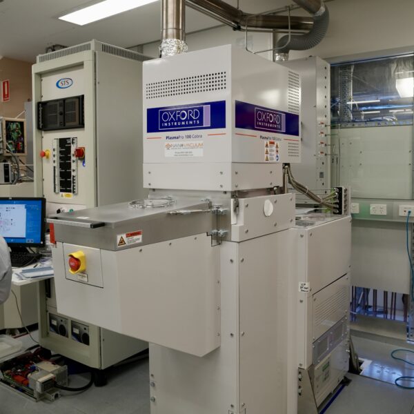
| Location | UNSW – West Lab (Grey Area) |
| ICP Power | 1800 W |
| Target power | 600 W |
| Gases | Ar, O2, CHF3, CF4, SF6, C4F8, He |
| Bosch process | YES |
| Substrate size | 4” |
| Electrostatic Clamp | YES |
Disco DAD3240 dicing saw
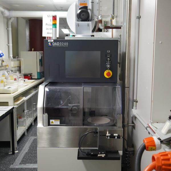
| Location | UNSW – Lower East Lab (Grey Area) |
| Table size | 8″ |
| Maximum wafer size | 6″ |
| Available blades | Si with 0.8mm exposure, and 0.035mm kerf |
| Si with 1.1 mm exposure, and 0.06mm kerf | |
| Glass up to 2mm thick with 0.2mm kerf | |
| Sapphire up to 2mm with 0.2mm kerf | |
| Quartz up to 2mm with 0.15mm kerf |