| Location | UNSW – Upper East Lab (White Area) |
| Wafer sizes | Up to 200 mm by 200 mm, 15 mm max. thickness |
| Light source | 365nm |
| Avail. resolutions | 0.5 µm, 0.7 µm, 1 µm, 2 µm and 5 µm at 365 nm |
| Greyscale levels | 256 levels |
Lithography
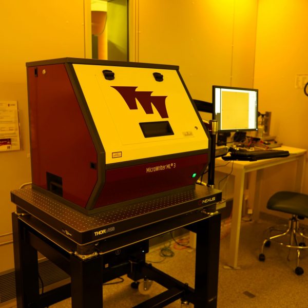
DMO MicroWriter ML3 Pro
Dry Film Laminator Fortex FL-0305-01 *
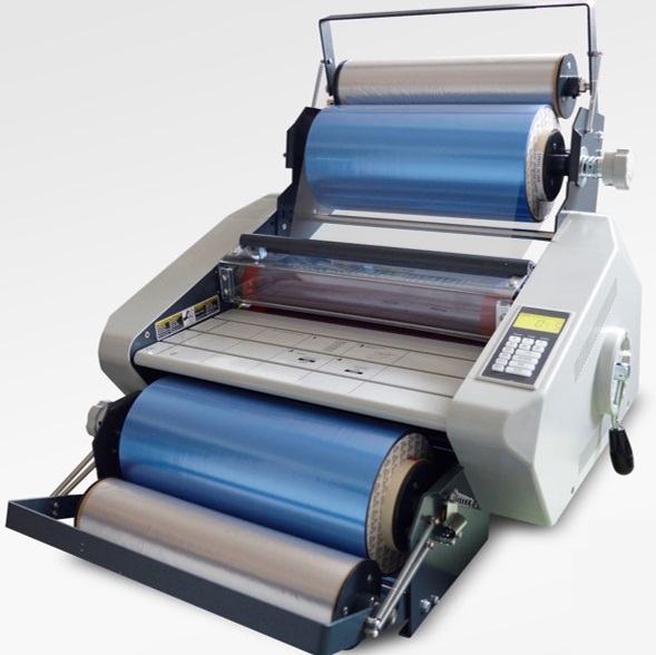
| Purpose | Uniform resist coverage and an alternative to thick liquid resist spin coating; the material feed type is an automatic roll of film and pre-cut sheets |
| Location | Photo-Lithography Bay, RPF Cleanroom |
| Material systems | Substrate material compatibility: wafers (silicon, glass, sapphire), brass, foils, steel, PCB |
| Scale / volume | Substrate thickness: up to 4mm; substrate size: from 5mm x 5mm up; 305mm x up to any desired length |
| Specs / resolution | Compatible with all dry film thickness range, but RPF stocks 50µm, 100µm, 200µm, and 500µm |
| * Not an ANFF-supported tool; access is available – refer to Access Fees schedule |
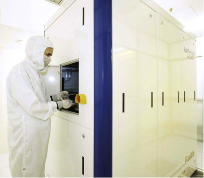
EBL Elionix ELS-F125 *
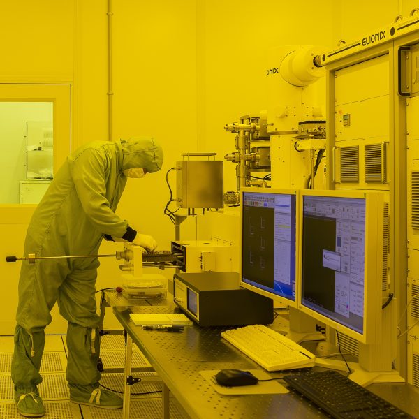
| Purpose | The Elionix electron beam lithography system has an acceleration voltage of 125kV and is capable of patterning high resolution features |
| Location | E-Beam Bay, RPF Cleanroom |
| Material systems | EBL resist coated wafers |
| Scale / volume | Accommodates small samples up to 6 inch wafers |
| Specs / resolution | 2nm beam diameter at 500pA beam current; dynamic focus and stigmatism adjustment; maximum 500um write field; field stitching error smaller than 20nm; overlay alignment better than 20nm |
| * Not an ANFF-supported tool; access is available – refer to Access Fees schedule |
Laser Writer Heidelberg DWL 66+
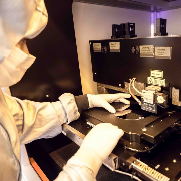
| Purpose | Direct write laser lithography system capable of high resolution and grayscale patterning; UV laser direct-write system at submicron resolution for quick prototyping |
| Location | Photo-Lithography Bay, RPF Cleanroom |
| Material systems | Photoresist coated substrates with up to 6mm thickness |
| Scale / volume | 375nm laser wavelength; accommodates up to 9 inch wafers; |
| Specs / resolution | 800nm; maximum write area 200mm x 200mm; multiple write modes – capable of achieving submicron features with highest resolution |
Mask Aligner EVG 610 *
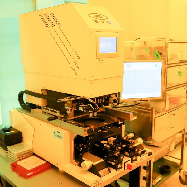
| Purpose | A photolithography tool that supports top and back sides mask alignment and can pattern with feature size in micron; vacuum contact, soft contact, proximity exposure modes |
| Location | Photo-Lithography Bay, RPF Cleanroom |
| Material systems | Photomasks and photoresist-coated substrates |
| Scale / volume | Photomask sizes: 4 inch, 5 inch, and 7 inch; substrate size: 2 inch, 4 inch, and 6 inch |
| Specs / resolution | Vacuum contact: 1 – 1.5um; soft contact: 1.5 – 3um; proximity: >3um |
| * Not an ANFF-supported tool; access is available – refer to Access Fees schedule |
Maskless Aligner Heidelberg MLA100 *
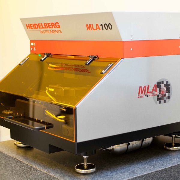
| Purpose | A fast-speed maskless alignment photolithography tool that patterns feature size down to 2um; UV LED direct-write system for feature sizes at the micron level |
| Location | Photo-Lithography Bay, RPF Cleanroom |
| Material systems | Photoresist coated substrates with up to 6mm thickness |
| Scale / volume | 365nm LED wavelength, fast writing speed; accommodates up to 6 inch wafers |
| Specs / resolution | 2um; maximum write area is 125mm x125mm |
| * Not an ANFF-supported tool; access is available – refer to Access Fees schedule |
MJB3 Mask Aligner
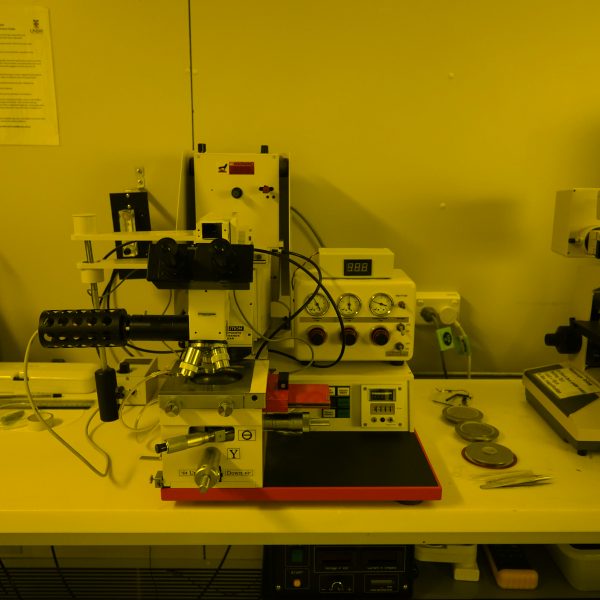
| Location | UNSW – Lower East Lab (White Area) |
| Sample holder size | From small chips up to 3” wafers |
| Mask holder size | 4” square |
| Exposure modes | Vacuum, soft contact, hard contact |
| UV lamp spec | 365nm, 10 mW/cm2 |
NMP Bath (photomask cleaning)
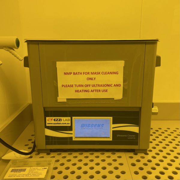
| Location | UNSW – Lower East Lab (white area) |
| Constant temperature bath | NMP at 80C |
| Other capabilities | ultrasonic |
| Mask size | up to 5” |
Spin coater (lower east)
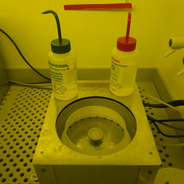
| Location | UNSW – East lab (White Area) |
| Sample size | Small chips up to 4” wafers |
| Spin speed | Up to 8000 rpm |
Spin Coater (West white)
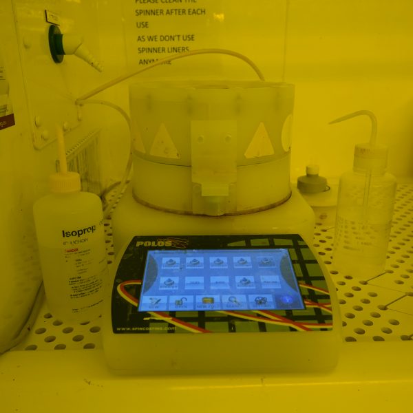
| Location | UNSW – West Lab (White Area) |
| Sample size | From small chips up to 6” |
| Max spin speed | 10k rpm |
| Max acceleration | 7300 rpm |
| Recipes | Multistep user programmable recipes |
Spin Dryer Delta 15
| Purpose | An automated single wafer substrate cleaning tool using DI water and compressed air |
| Location | Wet Process Bay, RPF Cleanroom |
| Scale / volume | 4 inch and 6 inch wafers; 4 inch, 5 inch, 6 inch, and 7 inch photomasks |
Wafer Track Processor Rite Track SVG88
| Purpose | A fully automated system for spin coating, HMDS application, baking, and development |
| Location | Photo-Lithography Bay, RPF Cleanroom |
| Material systems | Auto dispense of resist – standard SPR660, and another type; MF26 developer |
| Scale / volume | Throughput of up to 60 wafers per hour; accommodates 3 inch, 4 inch and 6 inch wafers |
| Specs / resolution | Capable of running 25 wafers at a time; the system is well suited to batch scale production, providing high process performance and consistency in coating and development |
Raith 150TWO Electron Beam Lithography System
| Location | UNSW – West Lab (White Area) |
| Sample size | From small chips up to 6” |
| SEM | ZEISS |
| Column | Gemini 0-30kV |
| Apertures | 7.5 10 15 20 30 60 120micron |
| FBMS | Available |
| Laser Height Sensing | Available |
| Focusing during exposure | By Column or by Stage Adjustment |
| Stitching Write Fields capability | Available |
| Smallest step size | 2nm |
| Beam shape | Spot |
| Minimum feature size | < 20nm |
| EBL resists available | Positive PMMA 950k, CSAR 9% and 18%, negative Ma-N2403 |
| Detectors | In-lens and SE |
Raith Pioneer TWO
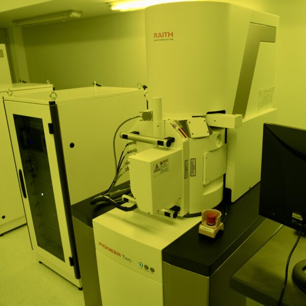
| Location | UNSW – West Lab (White Area) |
| Sample size | From small chips up to 2” |
| SEM | ZEISS |
| Column | Gemini 0-30kV |
| Apertures | 7.5 10 15 20 30 60 120micron |
| Laser Height Sensing | Available |
| Focusing during exposure | By Column or by Stage Adjustment |
| Stitching Write Fields capability | Available |
| Smallest step size | 2nm |
| Beam shape | Spot |
| Minimum feature size | < 8nm |
| EBL resists available | Positive PMMA 950k, CSAR 9% and 18%,
negative Ma-N2403 |
| Detectors | In-lens and SE |
Karl Suss MA6 mask aligner
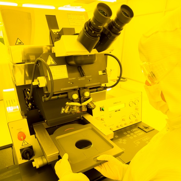
| Location | UNSW – West Lab (White Area) |
| Light source illumination | i-line (365nm) |
| Light Intensity | 10 mW/cm2 |
| Resolution | Down to 1 um
(depends on substrate size and flatness, resist type and thickness, and cleanroom conditions, and therefore, might vary for different processes) |
| Substrate size | Pieces from 5x5mm2, to 6” wafer |
| Photomask size | 4”, 5” and 7” |
| Exposure modes | Contact (Soft, Hard, Vacuum, Low vacuum)
Flood exposure |
| Alignment method | Top Side alignment (TSA)
Bottom Side alignment (BSA) |