| Purpose | A spindle dicing system that offers customizable and/or full-automatic dicing solution |
| Location | RPF Lab 3021 |
| Material systems | Wafers, silicon, glass, ceramic |
| Scale / volume | Capable of cutting semiconductor wafers, silicon, glass, ceramic up to 6 inches |
| Specs / resolution | High accuracy up to 1µm |
| * Not an ANFF-supported tool; access is available – refer to Access Fees schedule |
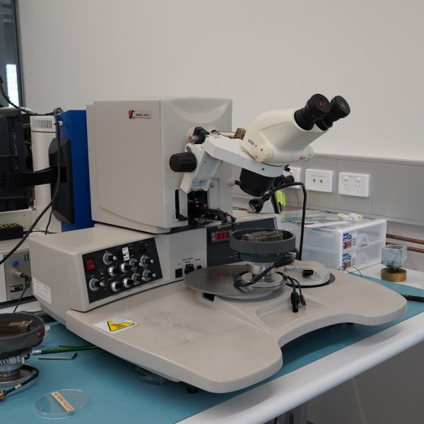
Packaging
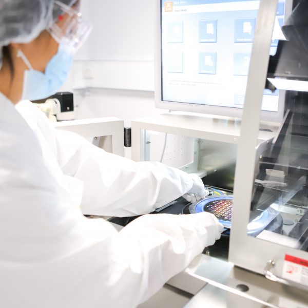
Dicing Saw ADT 7122 *
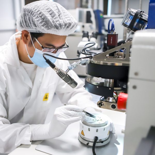
Die Bonder Fine Tech Lambda
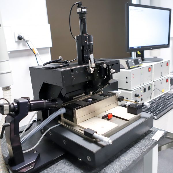
| Purpose | The die bonder provides sub-micron precision die attach and advanced flip-chip packaging capabilities |
| Location | RPF Cleanroom |
| Material systems | Epoxy / adhesive; formic acid; thermo-compression; thermo-sonic bonding |
| Scale / volume | Heated stage accommodates up to 50mm x 50mm samples; maximum chip size for the bonder pick is 15mm x 15mm |
| Specs / resolution | Precision placement and alignment; thermo compression; ultrasonic or thermosonic bonding, formic acid, adhesive dispense module |
Electrical Probe Station Suss PM 5
| Purpose | 4 probe DC probe station for measuring electrical properties of materials and devices |
| Location | RPF Lab 3021 |
| Scale / volume | Substrate size up to 6 inch wafer |
| Specs / resolution | Can heat substrate up to 120°C during measurement |
F&S Bondtech 53XX BDA Bonder
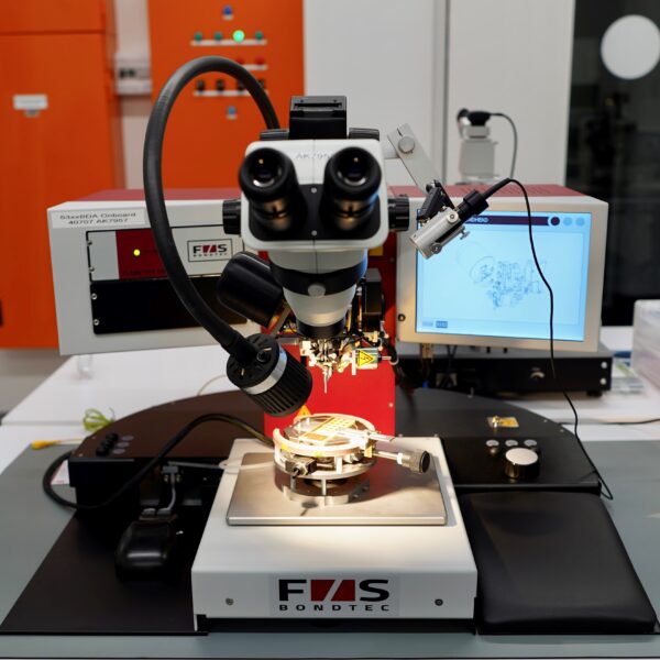
| Location | UNSW – South Lab (Test Area) |
| Configuration | 25 μ |
| Bondhead Z: | 60mm; step of 1 μm |
| Standard work height | 70mm |
| Manipulator in X and Y: | 18x18mm complies |
| Two-channel ultrasonic generator | 100-105 kHz 2.5 – 5 W |
| Wire guide | 90 °, 2 “wire coil |
K and S Al Wedge Bonder
| Location | UNSW – South Lab (Test Area) |
| Wire material | Al, 25 microns diameter |
| Bonding modes | 45 deg, manual, semi-automatic (Z-axis) |
Karl Suss Manual Wafer Scriber
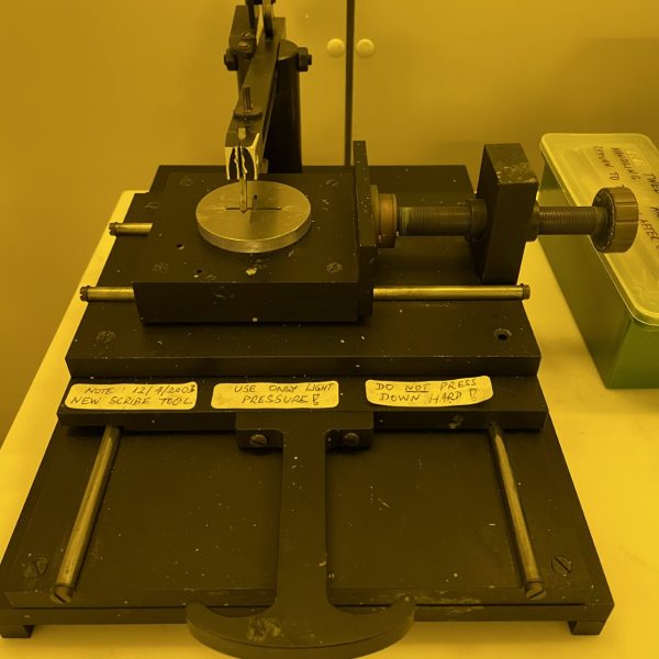
| Location | UNSW – Upper East Lab (White Area) |
| Wafer size | Small pieces up to 100 mm |
| Scriber tip | Diamond tip |
OEG MR200 diamond scriber
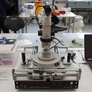
| Location | UNSW – South Lab (Test Area) |
| Wafer size | Small pieces up to 200 mm |
| Scriber tip | Diamond tip |
TPT HB10 Thermosonic Au Ball Bonder
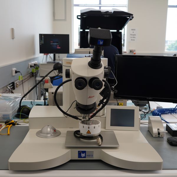
| Location | UNSW – South Lab (Test Area) |
| Wire material | Au, 25 microns diameter |
| Bonding modes | Manual, semi-automatic (Z-axis) |
| Options | Laser marker, video camera |
Wire Bonder TPT HB 100 *
| Purpose | The TPT wire bonder is capable of performing automatic and semi-automatic wire bonding with gold and aluminium wires |
| Location | RPF Lab 3021 |
| Material systems | Samples on PCB |
| Specs / resolution | Capable of manual, semi-auto and auto mode; wedge and ball bonding; deep access bond head |
| * Not an ANFF-supported tool; access is available – refer to Access Fees schedule |
Disco DAD3240 dicing saw
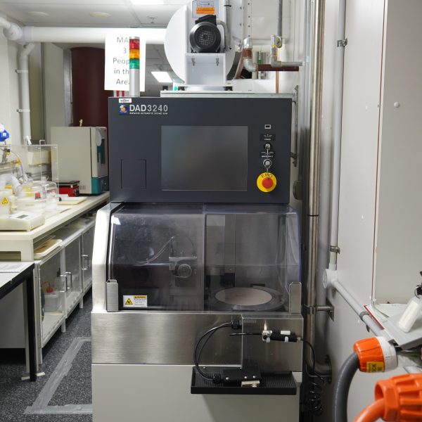
| Location | UNSW – Lower East Lab (Grey Area) |
| Table size | 8″ |
| Maximum wafer size | 6″ |
| Available blades | Si with 0.8mm exposure, and 0.035mm kerf |
| Si with 1.1 mm exposure, and 0.06mm kerf | |
| Glass up to 2mm thick with 0.2mm kerf | |
| Sapphire up to 2mm with 0.2mm kerf | |
| Quartz up to 2mm with 0.15mm kerf |